Miniaturization Trend
Contrinex 12th Dec 2022
Why miniaturize?
The ideal detector should be as precise as you want and infinitely fast, but close to zero in price and size. We will show in the following text first of all what it is possible to achieve today regarding size. Due to the ever-increasing intensive use of high-performance electronic machine controls, a larger concentration of sensors can be observed. This should not, if possible, oblige the machine manufacturer to modify the mechanics just to provide space for detectors, it would be in fact illogical that the use of detectors makes the mechanics bulkier, therefore more expensive and even possibly less effective. This automatically results in the requirement for smaller and smaller detectors. This particularly concerns the proximity detectors used in large quantities, which we will deal with in the following text.
Size reduction
The desired reduction concerns two aspects:
- In addition to the sizes described in the standard IEC 60947-5-2 for cylindrical proximity switches (04, MB, M12, M1B and M30), smaller sizes must be introduced, e.g. M4 and 03.
- In addition to the existing sizes in accordance with the aforementioned standard, the operating distance, which as we know is proportional to the diameter, must be enlarged. In this way, for a required operating distance we can use smaller devices. In the following text we will deal with the smaller construction; the enlargement of the operating distance will form the theme of a later publication.
Requirements

The miniaturization of an existing construction does not seem at first to be a particularly spectacular task. However, this is not the case for a whole series of reasons. One must first of all make sure that the user can install the miniaturized product without difficulty. He often wants to directly replace an existing device with a smaller one. This means that the latest device must display the same electrical characteristics as the larger device, in particular it must have the currently indispensable protection circuits (protection against short-circuits, polarity reversal protection, over-voltage protection, electromagnetic compatibility, etc.). Secondly, the user is generally unwilling to give up the comfort to which he has become accustomed in favor of miniaturization. The LED must be present. A high resistance to unfavorable environmental conditions is inevitable, the degree of protection IP 67 is required. The N.O and N.C. contacts, PNP, NPN and NAMUR configurations must be found in the offer. Highly flexible oil-resistant cables, as well as connector types, are required. Not only that, the devices must have a strong construction. This requires relatively thicker case walls. Further, the use of popular hybrid circuits on ceramic substrate is not recommended because of the increased risk of breakage due to the less favorable ratio between length and width. Miniaturization by reduction of the number of components is reducing the performances and is therefore a path which can not be followed. We still need to consider the economic aspect. The user is certainly ready to pay a little more for a smaller product; but if the large scale use of miniaturized devices is to be possible, these additional costs must be kept within certain limits. The use of expensive components and manufacturing processes is therefore immediately prohibited. On top of all this, despite the additional manufacturing difficulties, the reject rate must stay under control. Taking these explanations into consideration, we notice a miniaturization that takes the particular conditions mentioned into account is a demanding task.
Technique used
First of all, the circuit in question must be carefully analyzed. Solutions based only on discrete components are eliminated because of lack of space. As many functions as possible must be assured by an appropriate integrated circuit. A large number exist on the market, all of which nevertheless present more or less pronounced inconveniences. Experience shows that there is no hope of passing even one of these disadvantages on to the user in the form of restrictions. They must be eliminated by suitable additional discrete components. The use of ASICs (Application-Specific Integrated Circuit) is most often prevented by the large dimensions of the chip. An entirely specific integrated circuit could eventually be considered, but it can also only eliminate some of the discrete components.
Components
In a second stage, we must look for an appropriate outline of the components. We consider the smallest components available that can still be manipulated by SMD placers (table 1). The ferrite core presents a particular problem. Given that ordinary commercial cores are not suitable or even not available, we must take the more expensive option of a custom construction.
Resistors:
Chip resistors 0402 (1.0 x 0.5 mm) Micromelfs (2.0 x 1.0 mm)
Capacitors:
Ceramic capacitors 0402 (1.0 x 0.5 mm), 0504 (1.25 x 1.0 mm), 0603 (1.5 x 075 mm)
Semiconductors:
Diode chips (0.4 x 0.4 mm)
Zener diode chips (0.5 x 0.5 mm)
LED chips (0.4 x 0.4 mm)
Transistor chips (0.5 x 0.5 mm)
Integrated circuits as dies
Zener diode chips (0.5 x 0.5 mm)
LED chips (0.4 x 0.4 mm)
Transistor chips (0.5 x 0.5 mm)
Integrated circuits as dies
Substrate
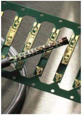
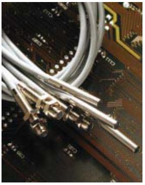
We must start by choosing a substrate, taking the assembly technique into consideration. Thin film substrates provide the highest density, but are abandoned for cost reasons. Thick film substrates could be used in principle; their inconvenience is a limited density (width and distance between the conductors, resistor surface required) and the high sensitivity to breakage of the ceramic. Epoxy substrates have shown themselves to be very appropriate. They unite high density, low costs, a low sensitivity to breakage and the possibility of embedded component mounting (important for the integrated circuit). The resistors cannot be printed as for hybrid thick film substrates; but this no longer plays an important role, with very cost effective SMD resistors available today and reduced assembly costs. An example of such a substrate is shown in figure 1; the dimensions are 17 x 2.5 mm. It is the mounting technique which is critical. For passive components (resistors and capacitors), SMD is unavoidable. Despite this, there is still an important obstacle to overcome from the everyday SMD constructions to a substrate for miniaturized proximity switches. A considerable investment to acquire the additional know-how cannot be avoided.
Assembly Technique
In order to mount very small SMD components with very close spacing (0.4 mm between components) on soldering surfaces surrounded very closely (0.1 mm) by conductors, the assembly technique must be perfectly mastered. First, the choice of soldering paste is important; because the best resolution and precision of the silk-screen printing must be achieved. The smallest impurity leads to problems, in particular if we must afterwards paste onto the same substrate (Chip-on-Board). Then, a suitable SMD placer must be chosen for the component placement. High speed operation is less important than to assure the precision and the manipulation of very small components. To achieve the best results, the machine must be used exclusively for the type of substrate for which it was originally set. It is unnecessary to emphasize that the soldering that follows is critical.
Chip-on-Board
Chip-on-Board technology is generally applied for semiconductors. Attention should be given here to the question of cost. The design rules for the substrate are critical; they influence notably the costs and the manufacturing wastage. The choice and the specifications of semi-conductors are also important: the layout and size of the bonding pads, type of metalization front and back, die thickness and packaging (loose, Waffle pack, Blue Film). The bonding procedure must be chosen with care; it's a matter of Goldball (thermo-compression) and Aluminium-Wedge. The shape of the loops and the angle of the bonding head respectively must be defined in a way as to avoid excessive height. If necessary, the chips will be mounted embedded. A separate chapter is devoted to the encapsulation of pasted semiconductors, which has a substantial influence on the reliability of the assembly.
Technical characteristics:
(In accordance with IEC 60947-5-2)
Sensing range 0.6 mm ± 10 %
Hysteresis 5 % typ.
Polarity PNP, NPN, NAMUR
Contact N.O., N.C.
Voltage range 10 ... 30 VDC
Ripple content 20 % max.
Output current 100 mA max.
Output voltage drop 2.0 V max. at 100mA
Current consumption 10 mA max.
Switching frequency 5000 Hz max.
Operating temperature range -25 T +70 0C
Temperature drift ± 10 % max.
LED Built-in
Voltage reversal Built-in
Power-on reset Built-in
Protection degree IP 67
EMC - protection:
IEC 60255-5 1 kV
IEC 61000-4-2 Level 2
IEC 61000-4-3 Level 3
IEC 61000-4-4 Level 2
IEC 61000-4-2 Level 2
IEC 61000-4-3 Level 3
IEC 61000-4-4 Level 2
Coil
A difficult phase is still the fixation of the ferrite core and the coil, as well as the soldering of the coil wires. Here, it is practically impossible to automate. It is necessary to have an ergonomic workplace and qualified personnel who are well trained and benefit from excellent vision, a steady hand and nerves of steel.
Potting
The potting of the proximity switches is an always necessary, but not much appreciated operation. It is not any different for miniature devices. In addition, the work must be carried out with great precision and cleanliness. For a good reliability in difficult operational conditions, it is essential to do the potting in a vacuum in order to avoid air bubbles being trapped. This is a condition essential for the desired long-term reliability (formation of micro-climates, corrosion).
Quality
The production of miniature detectors can only be mastered by the perfect enforcement of a consistent test philosophy. Already at the time of substrate design and the choice of components, the testing aspects must be considered, even if it is a matter of apparently simple elements. In the production, the principle: one operation - one test - next operation - next test, etc., must be absolutely respected. To this effect, complex methods are needed, since due to the small dimensions of the product, current test systems available on the market cannot be used. Everything must be designed and built by the manufacturer himself. To achieve a reduced reject rate, the test must, if possible, immediately follow the operation, in order to intervene as soon as possible. Repairs are often not possible because of the tight construction. The quality control of miniature devices operates on the same principle as for larger devices. To reach the best possible reliability, the devices are additionally subjected to thermal cycling (5 cycles from -25 °C to +B0 °C and back again). Furthermore, the functions are also verified at the temperature extremes.
Results
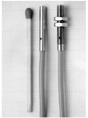
The smallest complete proximity switches in series production today have an outer diameter of 3 mm or a fine M4 thread and a body length of 22 mm (figure 2). These devices are produced in accordance with the principles set out, and they are indistinguishable from larger types by their performance, apart from their size and operating distance (table 2). A glance at the substrate used is offered by figure 2; the dimensions are 2.5 x 17 mm. These devices have been on the market for a number of years already and are in use in a considerable quantities. Experience until now shows that their use is entirely problem free and they open up new possibilities for manufacturers in cases where space is critical. Over and above their small size, advantage can be taken of some of the following properties: better reproducibility, better resolution (e.g. for scanning toothed wheels with modules going down to 1.5 and coding disks), lightweight and high switching frequency (5 kHz and over).
12th Dec 2022